Overview

From millimeter (mm) to nanometer (nm) has been a long and stupendous research work that has been changing our day to day life and experience. Nanotechnology is focused on the engineering and the physical properties of small structures. Therefore techniques that have sensitivities at a scale of 0.1 nm to 1000 nm are required to study these structures.

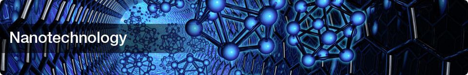
Growing Nano-layers: We provide turnkey & state of art technical solution for the development & production of Carbon Nano Tubes (Single Wall & Multi Wall cnts), Graphene, nanofibers and nanowires. These innovative systems are based upon Thermal CVD and patented DC Pulsed plasma-enhanced processes using Showerhead technology for Wafer scale device development.

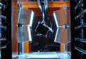
There are many other techniques to grow nanoscale thin layers of gan, gaas, Si, SiC, Metals & Dielectrics. These are Sputtering, MBE, CVD and Spin coating etc. Please go to Thin Film section.

Write with Nano-scale resolution: We specialize in nano-scale lithography with great ease together with nano-engineering tools to develop special Nano and Micro Mech Systems. I.e NEMS/MEMS and sensors.

We also provide Optical Lithographic equipment employing NIL technology (Nano-Imprint technology) in Mask Aligners that delivers ultra precise, front side, sub-micron & Nano scale patterning & alignment. Its flexible design allows printing on various substrates Nanoimprint module system is a modular add-on that can be used on any mask aligner.

To complement the Micro to Nano scale device development, we also offer Laser Writer which is used to directly write sub-micron patterns onto the substrates.

Another technique to Milling the nanoscale structure is Plasma Reactive Ion Etching. There are many techniques to Etch/Mill/Clean the layers. E.g. Inductively Coupled Plasma RIE, ECR RIE & parallel plate Plasma etchers.

Measuring with Nano-scale precision: After producing the Nano-scale devices, we also offer metrology solution with micro- and nanometer resolution.The award-winning measurement systems employ non-contact, non-destructive White Light and Chromatic Light Interferometer technology to collect data about the topography, structure, step height, roughness, wear, thickness and many other parameters of customer’s products.

Our Partners

MOCVD Equipment, OVPD

Spin Coaters & Spin Processors

Mask aligners, UV exposure systems, UV light sources, Solar

Laser Lithography equipment

CVD System, Dry Etching System, Dry Cleaning System

Crea Tec Fischer & Co.

Ion Beam Services S.A

Quick Query

Case Studies

  • Siliconizing of industrial fuses using UV curing

    The client is a multinational company with revenues of $5.4 billion in 2011 that

     view case study
  • Radtech India 2014 -UV/EB India Market Potential

    We are a 30 year old company serving the high technology sector of the Indian su

     view case study
  • UV Curing Of Adhesive In Hand Watches

    The client is a designer and manufacturer of watches, jewellery and other luxury

     view case study
  • UV Siliconizing Of Industrial Fuses

    The client is a multinational company with revenues of $5.4 billion in 2011 that

     view case study
  • Advancements in Carbon Fiber Processing

    Composites World, San Diego 2010 December 8, 2010

     view case study
  • A Highly Flexible Carbon Fiber Research Facility

    Intertech PIRA GOCarbonFiber 2011 October 5, 2011

     view case study
  • Thermal Processing Optimization

    Rotary furnaces are the go-to technology for high temperature processing of powd

     view case study
  • High Temp Powder Processing Advancements

    Rotary furnaces are the go-to technology for high temperature processing of powd

     view case study
  • Developing Thermal Processes

    Thermal processing is typically the most energy intensive portion of a materials

     view case study
  • Advanced Reactor System for Molybdenum

    Extensive investigation in the two-stage hydrogen reduction process for fine mol

     view case study
  • UV Curing on Mobile Phones

    The client is a multinational company, with net sales of over EUR 700 million in

     view case study
  • Optical fiber manufacturing

    The client is an Indian manufacturer and one of the world leaders in manufacturi

     view case study
  • Developing Advanced Carbon Fiber in India

    Nina Hsu Director, Government Relations & Business

     view case study
View All

Blog@Simco

UV coating cures and is chemically crosslinked. This provides for a coating film which has much high...

read more

Ultraviolet (UV) curing is a photochemical process in which high intensity UV is used to instantly c...

read more
View All

News and Events

  • Field-upgradeable eight-color laser engine Read More

  • Seminar on “Modular electron beam engines for R&D and Production ” -by Dr. Gregor Hommes on 2nd July 2015, Time : 10:30 am, Location : Committee Room, Department of Textile Technology, IIT Delhi Read More

  • Seminar on “Modular electron beam engines for R&D and Production ” -by Kaspar Zimmerli and Dr. Gregor Hommes on 30th June’2015, Location: Primrose Hall, The Regenza by Tunga Hotel, Vashi Timings: 10am- to 12pm Read More

  • Focusable Collimators for Coupling Light out of the Fiber Read More

  • IR Sensor Card / Low Power 5 – 20 μm Read More

  • IR Sensor Card / Low Power 1.5 – 5 μm Read More

  • Detector Screens for Wavelengths from 1.5 μm to 20 μm Read More

  • New Production Plant for PbS and PbSe Detectors Read More

  • Visit us @ “DAE-BRNS National Laser Symposium (NLS-23)” taking place on December 3rd to 6th 2014 Read More

  • Visit us @ “National Workshop on Fluorescence and Raman Techniques – 2014” taking place on December 15th to 19th 2014 (For more information visit www.fcsworkshop.in/ ) Read More

View All

© 2014 Simco-Groups. All rights reserved.